theafterparty
n00b

- Joined
- Apr 26, 2020
- Posts
- 5
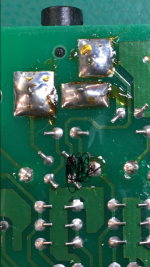
I just did a recap on my AES 3-5 and as I was removing a cap near the headphone jack, I realized there was a blob of solder joining at least two pins, maybe three together (see pics). To my eyes, my motherboard appears to be pretty stock as the factory glue was still there on what appeared to be original caps, and was in full working condition except for a few visual glitches here and there which after some research, I determined to be signs of old caps needing replacement.
Anyway I removed the blob of solder because I figured that was the safest move, and now my AES boots to a blue screen after a brief black screen but has audio and appears to be running the game. My thought on the blue screen is that it's actually just my projector not detecting proper signal and it's my projector's blue screen and not necessarily the Neo's if that makes sense.
Was this blob of solder the culprit and just needs replacing, or did I most likely botch some part of the display capacitor area? I made pretty neat work of it all, but I know those traces are pretty small.
My money would be on the solder blob except that it's on the audio side of the board, however I only know just enough about signal flow and traces to hopefully be asking the right questions. Thanks for any info.
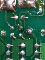
(Solder blob is represented by black lines in pics. Area is right below the headphone jack. Second picture is a close up of the first.)
Anyway I removed the blob of solder because I figured that was the safest move, and now my AES boots to a blue screen after a brief black screen but has audio and appears to be running the game. My thought on the blue screen is that it's actually just my projector not detecting proper signal and it's my projector's blue screen and not necessarily the Neo's if that makes sense.
Was this blob of solder the culprit and just needs replacing, or did I most likely botch some part of the display capacitor area? I made pretty neat work of it all, but I know those traces are pretty small.
My money would be on the solder blob except that it's on the audio side of the board, however I only know just enough about signal flow and traces to hopefully be asking the right questions. Thanks for any info.
(Solder blob is represented by black lines in pics. Area is right below the headphone jack. Second picture is a close up of the first.)