Good job with the pics!
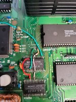
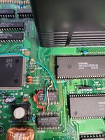
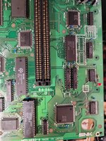
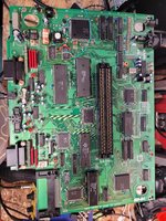
Now I can spot that the BIOS was socketed, the 68k as well, then a RAM IC (top right of the board) was either reflowed or replaced..
Trace repair was done on the BIOS as well.
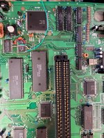
Those jumper wires for the SRAM ICs next to the reset button are way to big and dodgy soldered, 30 or 28 AWG Kynar is better suited.
That whole jumpers need to be redone.
Was that you or did you get the PCB like this? I'm asking because if you want tips for soldering, you can get them here
")
However, I will tell everyone that NeoGep HW, like Multislots or AES, are absolutely not what people should start practising on..
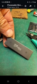
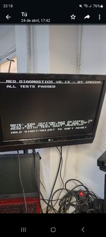
In any case, get a DIAG BIOS burned, that will help a lot, the BIOS is already socketed.
TBH there is some rotten traces, lots of rework, I'd risk saying "someone with experience will be able to save it", for a novice its not the right place to start, those SRAM ICs next to the reset button need to be redone, very easy to rip the traces off and make things worse..

 20230425_195722.jpg1.5 MB · Views: 5
 20230425_195736.jpg1.5 MB · Views: 6
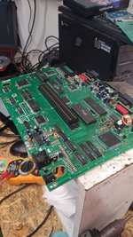 IMG-20230425-WA0091.jpeg1.2 MB · Views: 7
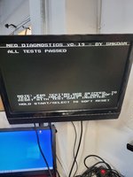 16824966628136875785368048024142.jpg1.4 MB · Views: 4
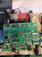 16824966774302586131494492894061.jpg1.9 MB · Views: 4
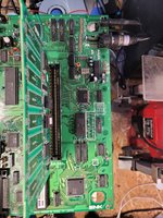 16824966902403120017803775302960.jpg2.2 MB · Views: 4
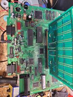 16824967018948804875076452040672.jpg2.4 MB · Views: 6
 20230426_165710.jpg1.9 MB · Views: 6
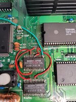 20230426_192936.jpg1.9 MB · Views: 4