MVS Z80 error

Hairy Otter

New Challenger
Joined
Aug 11, 2012
Posts
53
I'm trying to fix a MV2F with a Z80 error.
First I swaped the Z80 and the SM1 with those from a working board. The working board still working, the broken one is still broken.
Then I got my new toy, the logic analyzer. Give this a try to find the problem. Now I found D1 on all components acting strange. The first few bits go as on the good board, but then this get very quiet for a while.
Where is it supposed to get this data? Does this come from the 68k via the NEO-C1?
The SD1 (Pin 75) give's the same result. D9 (from the 68k) give other results, but so do D8-15 compared to SD0-7.

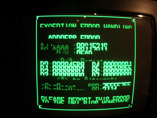
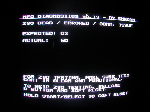
I've tested the board with the SMKDAN bios with the following message:

z80 dead/ errored / comm. issue
expected: C3
actual: 84
what does this mean?
 
Last edited:

GadgetUK

Ace Ghost Pilot
Joined
Sep 27, 2013
Posts
1,323
Could be the RAM associated with the Z80. It's expecting 11000011 in binary, and getting back 10000100 which is very different - ie. doesn't look like 1 bit invalid etc. I would take a look at the MV1FZ schematics and focus on checking traces between Z80, Yamaha and the sound RAM.
 

Hairy Otter

New Challenger
Joined
Aug 11, 2012
Posts
53
When I put in a unibios to see if there are more problems with the board, there appears to be a problem with one of the addresses. It looks that the A2 from the C-ROM is stuck. this makes a mirrored sets or 4 rows. As explained in: wiki.neogeodev.org
This makes it hard to read the text on the screens.
Also the cross hatch looks strange?
14612264644_7faec4fbde.jpg

With game inserted:
14613810102_e28f8e5067.jpg

14611122481_b2ddc47983.jpg


The same problem arises with the SMKDAN bios. : While the text is difficult to read in the first raport, it gives: ALL TESTS PASSED
14591267166_2ba5d3167a.jpg

But here are the z80 test page a smaller case letters, so that everything is legible.
14613757812_646d3f30b7.jpg
 

mjs256

Kula's Candy
10 Year Member
Joined
Apr 1, 2010
Posts
292
It looks like this board has more wrong with it than whatever is causing the Z80 error. The Z80 error means there is something wrong with the sound hardware. The graphics issue appears to be something entirely different. Like you said, it does look like an address issue. I would try starting it up with SMKDAN's bios and hold A+B+C+D so that you can go through each test individually and see if you get more insight.

It looks like it is showing double-size letters sometimes when it should be showing single-size letters. Check the IC that holds the text font data (I am not sure where it is stored but I would guess it is either in the SFIX ROM or LO ROM - maybe someone else here knows for sure). Use your logic probe to look for differences in the logic states of the address lines between your working board and the non-working one.

Since it gets the correct text data some of the time the issue is probably not with the text ROM itself, but if you find a discrepancy there then you should be able to trace it back to the source of the problem.

I would fix the graphics issue first and worry about the Z80 error later - you can't really trust anything that the system is trying to tell you until the graphics glitch is repaired.

Good luck!
 

Hairy Otter

New Challenger
Joined
Aug 11, 2012
Posts
53
It looks like this board has more wrong with it than whatever is causing the Z80 error. The Z80 error means there is something wrong with the sound hardware. The graphics issue appears to be something entirely different. Like you said, it does look like an address issue. I would try starting it up with SMKDAN's bios and hold A+B+C+D so that you can go through each test individually and see if you get more insight.
With SMKDAN's bios it gives: ALL TESTS PASSED. Only unibios give's errors. And while going trough the test screens I found the inputs also not working as they should. The player2 UP seems stuck some other player2 inputs don't respond. If I press down the up goes to 0 for short time. I tested the pull up resistor, they are all ok. So it seems the board has some major issues. Maybe the NEO-C1 is the problem. It seems to handle both inputs as well as the Z80 communication.
Thanks for your luck, I will need it!
 
Last edited:

GadgetUK

Ace Ghost Pilot
Joined
Sep 27, 2013
Posts
1,323
Based on what you've said about control inputs makes me suspect the Neo-C1 chip. Check the data lines from C1 chip aren't shorted to each other, and check inputs aren't shorted as well (at the point the signals enter the C1). If there are no shorts there I would hazard a guess that the C1 needs replacing. Haven't got access to schematics at the moment - check if C1 connects to any of the graphics hardware. Someone just mentioned it can relate to Z80 so it could all be related to a faulty C1.
 

Hairy Otter

New Challenger
Joined
Aug 11, 2012
Posts
53
@mjs256: After I had studied the default fix layer tile set, I came to the conclusion that A8 was stuck on high. So I followed the A8 to the NEO-IO chip and the logic analizer confirmed my suspicion. As a test I lifted the corresponding pin of the NEO-IO. Now I can change the small letters back to normal by holding the pin A8 of the SFIX to 0. Only thing is that the top half of large letters now become small letters instead of top parts, the bottom half change from top parts to bottom parts. The crosshatch looks better to.
This needs to be fixed, but now I can at least read the error messages.

@GadgetUK: I am afraid that the NEO-C1 is indeed broken. So let's practice to swap a 100-pin SMD chip. The NEO-IO is no problem I think, as I already swapped a bunch of those 64 pin chips successfully.

Another question to the group:
Are the errors I see with the Unibios inserted and a card present errors about the communication between the board and the card? Or does this also tell something about the board itself?

Answering my own question: It does tell something about the board. Now I fixed the major problem of the board (the faulty NEO-C1) all error messages are gone.
 
Last edited:

GadgetUK

Ace Ghost Pilot
Joined
Sep 27, 2013
Posts
1,323
Since you've got an Neo-io problem, and a C1 problem (could also be contributing to the Z80 error), then I would guess there's been perhaps a slight over voltage or something similar. That's not definite but possible. I haven't looked at schematics, but if those two chips are linked in any way, it's possible that a fault in one has contributed to the other. Is that what you mean?
 

Hairy Otter

New Challenger
Joined
Aug 11, 2012
Posts
53
@GadgetUK: As I was pretty sure the NEO-IO was bad and it's an easy swap, I replaced it. Now I'm getting all good text in the screens. One step forward in having my first working 2-slot!
I'm not sure what made this board fail, as when I got it, it was in non working condition and I don't know anything about its history.

Now I'm trying to find the guts to replace the NEO-C1 as well. The only way to learn this is by doing it, I think. Trying on a total loss board doesn't confirm I did a good job, so this one maybe has to take one for the team. After all, I can try several times on the same board. As long i don't burn of any traces.
 

Hairy Otter

New Challenger
Joined
Aug 11, 2012
Posts
53
Again one step closer! I swapped the NEO-C1.
With my first try the board booted to a unibios error screen with only a partial frame around the screen. :( I wasn't sure the donor NEO-C1 was in working order as I took it from an other non working board.
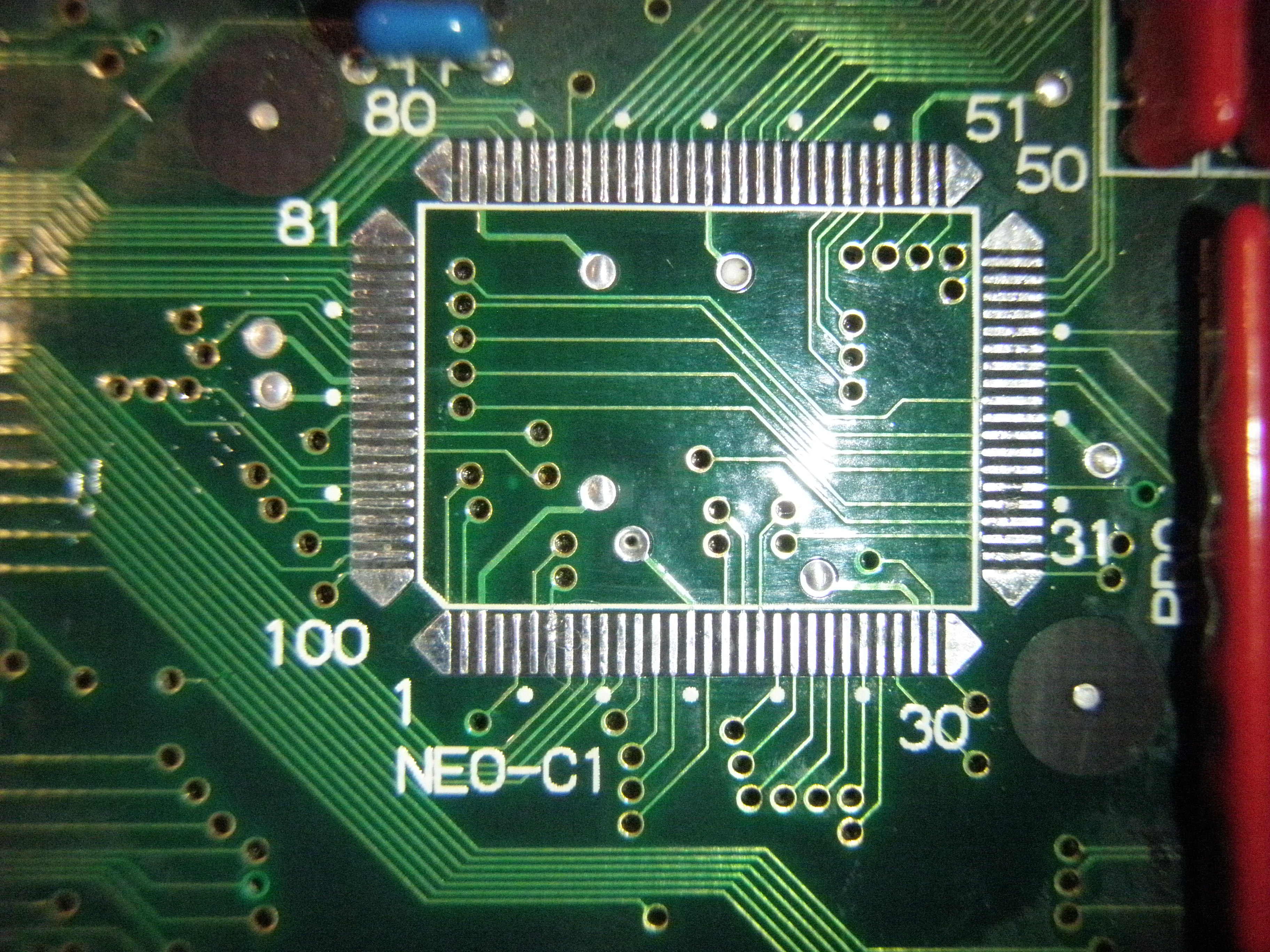
I checked for shortages or bad soldering but didn't find any. To be on the safe side, I reflowed all joints a second time and booted again. Tada! It's alive.

Sprites are all blocks, but the games are playable with good audio. This is a problem I can tackle, as the area around the battery has some serious leakage damage, so I'm sure there are some eaten traces and troughs.

For future reference I post a picture of the traces under the chip. Maybe someone can use it to trace the pins. (clickable for full view)


And just to show off my soldering skills: ;)


GadgetUK

Ace Ghost Pilot
Joined
Sep 27, 2013
Posts
1,323
Sweet! Great job, fantastic progress! For anyone else finding this post - I uploaded a vid on YouTube late last year covering the removal and replacement of the neo-c1 chip.

You've done a great job there! Hopefully it will be 100% soon!
 

mjs256

Kula's Candy
10 Year Member
Joined
Apr 1, 2010
Posts
292
Nice job on replacing the NEO-IO and NEO-C1! I recently repaired an MV-2F with battery leakage damage. I have all of the pin connections on the two NEO-257 ICs and the NEO-ZMC2, as well as the typical logic states on those when a game is running, so let me know if you want that information.
 

Hairy Otter

New Challenger
Joined
Aug 11, 2012
Posts
53
Nice job on replacing the NEO-IO and NEO-C1! I recently repaired an MV-2F with battery leakage damage. I have all of the pin connections on the two NEO-257 ICs and the NEO-ZMC2, as well as the typical logic states on those when a game is running, so let me know if you want that information.
This info would be great! If you like to share with us all, you can post this here. If you want to keep this personal you can PM me.
Without your info this could be a long job, as I don't have a working 2-slot.

Or maybe I beter open a new thread to keep things organized for future users?

There wasn't that much of a struggle.
Tested the data inputs to the ZMC2, all tested ok. So the NEO-257 must be ok.
Tested outputs GAD0~GAD3 & GBD0~GBD3 all stuck low? :scratch:
And with already two chips fried I took a gamble and swaped this too. Et voilà, audio and video as it should be. :buttrock:

It seems this bord has had some major over voltage?:very_ang:

@mjs256: Still want the info about the NEO-257 ICs and the NEO-ZMC2, for future reference. I want to fix as many MVS boards to preserve them for the future.
 
Last edited:

tonycawa

n00b
Joined
Jul 13, 2014
Posts
16
Awesome job, good read, hopefully I will never have to do this! Sounds like somebody hooked the board up to a power supply that was set to high.
 

Hairy Otter

New Challenger
Joined
Aug 11, 2012
Posts
53
Yet again! Z80 problems. After testing several games with success I stumbled on a game with some strange sounds. My puzzled-game makes strange noises. :blow_top:
Put in the diagnostics bios which tells me: M1 BANK ERROR 16K

So this epic journey isn't at its end.
 

GadgetUK

Ace Ghost Pilot
Joined
Sep 27, 2013
Posts
1,323
So close! Hope you can fix that bank error! Let us know you get on!
 

smkdan

Galford's Armourer
Joined
Dec 30, 2009
Posts
452
The bottom of my BIOS page has the pins to check for bank errors but I would also check Z80 A11~A14 to the CHA connector.

SDRD0 from NEO-D0 should pulse on every M1 bank swap which most games do constantly. I think you're almost done if this is the only thing left.

edit: forgot to mention since this is a 2F that these traces lead to NEO-E0, and then to each cart slot. See here.
 
Last edited:

mjs256

Kula's Candy
10 Year Member
Joined
Apr 1, 2010
Posts
292
Sorry that it is still giving problems. It sounds like you almost have it completely repaired. I have a working MV-2F that I can check with my logic probe if you want any comparisons.

Here are the pin connections and a (partly incomplete) list of logic states I have for the MV-2F which you asked for.

There may be more connections in addition to those indicated, but the connections shown should be sufficient to detect any lifted pins. Do not use a logic probe to check the state of pins connected directly to GND or +5V. Do that by checking for continuity between the pin and GND or +5V with the board off and disconnected. If there is continuity then you know the state will be L for GND and H for +5V and there is no need to verify it with a logic probe while the board is running (by doing so you run the risk of accidentally touching both a GND pin and a +5V pin, which is often right next to it, with the tip of your probe and then POW!).

I used this convention for the logic states:
L = continuous low state
H = continuous high state
B = switching between both low and high
LB = mostly low but occasionally switching to high
HB = mostly high but occasionally switching to low
N = no signal detected
* = requires explanation
? = the signal confused my logic probe
- = did not measure


Code:
MV-2F NEO-G0 CONNECTIONS
------------------------

pin  state  connection
---  -----  ----------
01     -    CRT2PRG08A
02     -    CPU pin 05
03     -    CPU pin 04
04     -    CPU pin 03
05     -    CPU pin 02
06     -    CRT1PRG05A
07     -    CRT1PRG06A
08     -    CRT1PRG07A
09     -    CRT1PRG08A
10     L    GND
11     -    CRT1PRG09A
12     -    CRT1PRG10A
13     -    CRT1PRG11A
14     -    CRT1PRG12A
15     -    CPU pin 01
16     -    CPU pin 64
17     -    CPU pin 63
18     -    CPU pin 62
19     -    No Connection
20     -    No Connection
21     -    CRT2PRG09A
22     -    CRT2PRG10A
23     -    CRT2PRG11A
24     -    CRT2PRG12A
25     L    GND
26     H    +5V
27     -    CRT1PRG13A
28     -    CRT1PRG14A
29     -    CRT1PRG15A
30     -    CRT1PRG16A
31     -    CPU pin 61
32     -    CPU pin 60
33     -    CPU pin 59
34     -    CPU pin 58
35     -    CRT2PRG13A
36     -    CRT2PRG14A
37     -    CRT2PRG15A
38     -    CRT2PRG16A
39     -    NEO-IO pin 28
40     -    CPU pin 09 / NEO-IO pin 32
41     -    No Connection
42     L    GND
43     -    CRT1PRG17A     
44     -    CRT1PRG18A
45     -    CRT1PRG19A
46     -    CRT1PRG20A
47     -    CPU pin 57
48     -    CPU pin 56
49     -    CPU pin 55
50     -    CPU pin 54
51     -    NEO-IO pin 27
52     -    CPU pin 09 / NEO-IO pin 32
53     -    CRT2PRG17A
54     -    CRT2PRG18A
55     -    CRT2PRG19A
56     -    CRT2PRG20A
57     L    GND
58     H    +5V
59     -    No Connection  
60     L    GND
61     L    GND
62     -    CRT2PRG05A
63     -    CRT2PRG06A
64     -    CRT2PRG07A
Code:
MV-2F NEO-257@J2.5 CONNECTIONS
------------------------

Logic states taken with Cyber-Lip in slot 1

pin  state  connection
---  -----  ----------
01     -    CRT2CHA26B
02     L    GND
03     L    GND
04     B    CRT1CHA19A
05     -    CRT2CHA19A
06     B    CRT1CHA19B
07     -    CRT2CHA19B
08     B    NEO-ZMC2 pin 15
09     B    NEO-ZMC2 pin 19
10     L    GND
11     B    NEO-ZMC2 pin 16
12     B    NEO-ZMC2 pin 20
13     B    CRT1CHA20A
14     -    CRT2CHA20A
15     B    CRT1CHA20B
16     -    CRT2CHA20B
17     1*   NEO-257@K2.5 pin 17 / NEO-F0 pin 39
18     L    GND
19     B    CRT1CHA21A
20     -    CRT2CHA21A
21     B    CRT1CHA21B
22     -    CRT2CHA21B
23     B    NEO-ZMC2 pin 17
24     B    NEO-ZMC2 pin 21
25     L    GND
26     H    +5V
27     B    NEO-ZMC2 pin 18
28     B    NEO-ZMC2 pin 22
29     B    CRT1CHA22A
30     -    CRT2CHA22A
31     B    CRT1CHA22B
32     -    CRT2CHA22B
33     L    GND
34     L    GND
35     H    +5V
36     B    CRT1CHA23A
37     -    CRT2CHA23A
38     B    CRT1CHA23B
39     -    CRT2CHA23B
40     B    NEO-ZMC2 pin 24
41     B    NEO-ZMC2 pin 28
42     L    GND
43     B    NEO-ZMC2 pin 25     
44     B    NEO-ZMC2 pin 29
45     B    CRT1CHA24A
46     -    CRT2CHA24A
47     B    CRT1CHA24B
48     -    CRT2CHA24B
49     -    No Connection
50     -    No Connection
51     B    CRT1CHA25A
52     -    CRT2CHA25A
53     B    CRT1CHA25B
54     -    CRT2CHA25B
55     B    NEO-ZMC2 pin 26
56     B    NEO-ZMC2 pin 30
57     L    GND
58     H    +5V
59     B    NEO-ZMC2 pin 27  
60     B    NEO-ZMC2 pin 31
61     -    No Connection
62     B    CRT1CHA26A
63     -    CRT2CHA26A
64     B    CRT1CHA26B

1* = L when accessing slot 1; H when accessing slot 2.
Code:
MV-2F NEO-ZMC2 CONNECTIONS
------------------------

Logic states taken with Cyber-Lip in slot 1
If two states are given, it alternates between states as the game cycles through intro/demo

pin  state  connection
---  -----  ----------
01     LB   NEO-B1 pin 046     
02     L    GND
03     LB   NEO-B1 pin 047
04     B    LSPC-A2 pin 065
05     LB   LSPC-A2 pin 147
06    LB/B  LS32@E2 pin 01 and 02
07    LB/B  LSPC-A2 pin 109
08     N    No Connection
09     B    LSPC-A2 pin 066
10    LB/B  NEO-B1 pin 053
11    LB/B  NEO-B1 pin 054
12     L    GND
13    LB/B  NEO-B1 pin 055
14    LB/B  NEO-B1 pin 056
15    LB/B  NEO-257@J2.5 pin 08
16    LB/B  NEO-257@J2.5 pin 11
17    LB/B  NEO-257@J2.5 pin 23
18    LB/B  NEO-257@J2.5 pin 27
19    LB/B  NEO-257@J2.5 pin 09
20    LB/B  NEO-257@J2.5 pin 12
21    LB/B  NEO-257@J2.5 pin 24
22    LB/B  NEO-257@J2.5 pin 28
23     L    GND
24    LB/B  NEO-257@J2.5 pin 40
25    LB/B  NEO-257@J2.5 pin 43
26    LB/B  NEO-257@J2.5 pin 55
27    LB/B  NEO-257@J2.5 pin 59
28    LB/B  NEO-257@J2.5 pin 41
29    LB/B  NEO-257@J2.5 pin 44
30    LB/B  NEO-257@J2.5 pin 56
31    LB/B  NEO-257@J2.5 pin 60
32    LB/B  NEO-257@K2.5 pin 08
33     H    +5V
34    LB/B  NEO-257@K2.5 pin 11
35    LB/B  NEO-257@K2.5 pin 23
36    LB/B  NEO-257@K2.5 pin 27
37    LB/B  NEO-257@K2.5 pin 09
38    LB/B  NEO-257@K2.5 pin 12
39    LB/B  NEO-257@K2.5 pin 24
40    LB/B  NEO-257@K2.5 pin 28
41    LB/B  NEO-257@K2.5 pin 40
42     L    GND
43    LB/B  NEO-257@K2.5 pin 43
44    LB/B  NEO-257@K2.5 pin 55
45    LB/B  NEO-257@K2.5 pin 59
46    LB/B  NEO-257@K2.5 pin 41
47    LB/B  NEO-257@K2.5 pin 44
48    LB/B  NEO-257@K2.5 pin 56
49    LB/B  NEO-257@K2.5 pin 60
50     ?    NEO-E0@K10 pin 51
51     N    No Connection
52     L    GND
53     L    No Connection
54     L    No Connection
55     L    No Connection
56     L    No Connection
57     L    No Connection
58     L    No Connection
59     L    No Connection
60     L    No Connection
61     L    No Connection
62     L    No Connection
63     L    GND
64     L    No Connection
65     L    GND
66     L    GND
67     L    GND
68     L    GND
69     L    GND
70     L    GND
71     L    GND
72     L    GND
73     H    +5V
74     L    GND
75     L    GND
76     L    GND
77     L    GND
78     L    GND
79    LB/B  NEO-B1 pin 044
80    LB/B  NEO-B1 pin 045
Code:
MV-2F YM2610 CONNECTIONS
------------------------

Logic states taken during the stock BIOS sound test

pin  state  connection
---  -----  ----------
01     L    GND
02     B    NEO-257@JH9 pin 40
03     B    NEO-257@JH9 pin 41
04     B    NEO-257@JH9 pin 43
05     B    NEO-257@JH9 pin 44
06     B    NEO-257@JH9 pin 55
07     B    NEO-257@JH9 pin 56
08     B    NEO-257@JH9 pin 59
09     B    NEO-257@JH9 pin 60
10     B    NEO-G0@K9 pin 18
11     B    NEO-G0@K9 pin 17
12     B    NEO-G0@K9 pin 16
13     B    NEO-G0@K9 pin 15
14     B    NEO-G0@K9 pin 05
15     B    NEO-G0@K9 pin 04
16     LB   NEO-G0@K9 pin 03
17     B    NEO-G0@K9 pin 02
18     L    GND
19     H    +5V
20     B    NEO-E0@F7.5 pin 31
21     B    NEO-E0@F7.5 pin 32
22     B    NEO-E0@F7.5 pin 17
23     B    NEO-E0@F7.5 pin 16
24     N    No Connection
25     N    No Connection
26     L    GND
27     ?    1 kOhm resistor@B2.5
28     ?    JRC4558D@B4.5 pin 08
29     B    YM3016 pin 08
30     B    YM3016 pin 07
31     1*   YM3016 pin 04
32     L    GND
33     H    NEO-D0@G11 pin 34
34     N    No Connection
35     L    NEO-E0@F7.5 pin 18
36     L    NEO-E0@F7.5 pin 19
37     L    NEO-E0@F7.5 pin 20
38     L    NEO-E0@F7.5 pin 21
39     N    No Connection
40     H    NEO-E0@F7.5 pin 26
41     L    NEO-E0@F7.5 pin 33
42     L    NEO-E0@F7.5 pin 34
43     L    NEO-E0@F7.5 pin 36     
44     L    NEO-E0@F7.5 pin 37
45     N    No Connection
46     H    NEO-E0@F7.5 pin 48
47     L    NEO-E0@F7.5 pin 38
48     N    NEO-G0@K9 pin 31
49     N    NEO-G0@K9 pin 32
50     N    NEO-G0@K9 pin 33
51     N    NEO-G0@K9 pin 34
52     N    NEO-G0@K9 pin 47
53     N    NEO-G0@K9 pin 48
54     N    NEO-G0@K9 pin 49
55     N    NEO-G0@K9 pin 50
56     2*   Z80 pin 16
57     HB   NEO-D0@G11 pin 49
58     HB   NEO-D0@G11 pin 47
59     HB   NEO-D0@G11 pin 48
60     B    Z80 pin 30
61     B    Z80 pin 31
62     H    +5V
63     LB   NEO-E0@K10 pin 53
64     LB   YM3016 pin 05

1* = alternates beteen B an LB during beep and in between beeps
2* = B at the beginning and end of each beep; otherwise HB
 

Hairy Otter

New Challenger
Joined
Aug 11, 2012
Posts
53
:crying:

Now Neo Diagnostics BIOS tells me all test passed! Including Z80.
The SDRD0 from NEO-D0 pulsed all the way to the cart, but after comparing the signal with a working board, this proved to be different. There seemed certain pulses not to come out of the NEO-D0. So I re-soldered the NEO-D0, with the result that the bank error was corrected.
But now my puzzled game doesn't give any sound at all? Tecmo world soccer '96 gives very distorted audio, so the amp is still ok, also in test screens there is audio? Both (and my two other test carts) work ok on my other boards so this isn't the problem. All boards give the same issues on both slots so I can rule out dirty slots.

When will this board surrender. I'll keep you all in the loop of my progress. All tips are still welcome.

@mjs256: Thank you for sharing your research with the group. There are certainly other users that can use it and I will definitely keep this information for future bugfixes.

Update: After I used mjs256's info and probed the ym2610, without any difference, I now have distorted audio with all my cards? Again a step, but not the finish.
 
Last edited:

Hairy Otter

New Challenger
Joined
Aug 11, 2012
Posts
53
I looked around on the net and stumbled across the Xian Xi site. Here is a tutorial about the MVS YM2610 to NEO-PCM Pinout. Here he tells: If you are experiencing screeching audio or missing sounds check for continuity with these.

So I took a closer look.
The A43-56 is linked between the two slots so its easy to access, but alas this compared to my working 4 slot.
The B41-56 I couldn't reach as they are in between the 2 boards :(
Now I slipped some paper between a pin and the cart on my working 4 slot and with some paper between the contact of a B49-56 pin there where similar issues. These pins lead the SDRAD signals to the NEO-G0@k9 on the 2 slot. With my logic probe I found activity on all the pins, but I couldn't compare it, as on my 4 slot I can't reach those pins while playing.
I took a chance and replaced the G0, with success! The board played as a charm.

But as I expected, after some test games and two game's in the board, the board resets in the middle of a game. It reboots twice and goes to the second slot game. This plays the intro and gets corrupted, reboots and start again until it reboots. Now The first slot goes to crosshatch. The second is corrupted.

I dropped in another G0, with less success this time. Both slots play, but with no sound. Yet another spare gave me other distortions?:angry:
As I don't have any spares left, I tried in the original. Back to the distorted audio as before, so I found the culprit! But this also takes this repair to a standstill.
Now I have to wait to find a good NEO-G0. I think I found my match with this board.
 
Last edited:

smkdan

Galford's Armourer
Joined
Dec 30, 2009
Posts
452
Are you completely sure the G0 swap caused the the resets and cross hatching? It makes sense for that G0 to cause undetected sound issues since all PCM data goes through it, but that's all it's used for (see the wiki pinouts).
 

Hairy Otter

New Challenger
Joined
Aug 11, 2012
Posts
53
Are you completely sure the G0 swap caused the the resets and cross hatching? It makes sense for that G0 to cause undetected sound issues since all PCM data goes through it, but that's all it's used for (see the wiki pinouts).

I do not doubt your expertise on MVS boards. But yesterday evening I made ​​several exchanges. Each time the same faults with the same chip. I can't explain, but maybe some internal short can cause the resets?
I have no means to test the chips "offline". But there is only one which causes these resets. With one game inserted in slot 1 it gave one reset very early in the boot, before the intro screen, then it goes to crosshatch. In slot 2 the game keeps playing into attract mode but there after a few seconds the game gets corrupted and the board resets. (maybe the watchdog doe this?) With two games inserted the board resets twice, similar to the slot 1 only situation, then goes to slot 2. Now he keeps skipping slot 1 and start only slot 2 until it resets and start slot two again?
This morning I discovered that the NEO-G0 is not only to be found on the 2 slot boards. And now I have a chip from a scrap 4-slot board and the 2 slot works fine.
He now is running a burn in test. :multi_co: Lets hope he keeps working, but either way, I've learned a lot by doing this repair. I now understand more about how the MVS works, and I honed my soldering skills to a new level.

Special thanks to all the people who helped me with this. Both through this board and through their homepages.
 

aha2940

AH, A, COLUMBIAN!,
Joined
Dec 15, 2013
Posts
2,528
Congratulations fixing your 2-slot man, fixing these things is part of ehat makes this hobby interesting IMHO. Also, you get a sense of achievement when you play on something you fixed yourself.

Regards.


Sent from my mobile device using Tapatalk
 
Top