Xmen pcb, video out of sync

ahcmetal

Super Spy Agent
10 Year Member
Joined
Aug 25, 2010
Posts
624
I'm having some back luck with my boards lately, I hooked up my xmen pcb to find that the image is scrambled and out of sync.
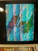
20170530_132049.jpeg

I picked up a Elenco LP-560 logic probe...no idea how to effectively use it...and found some schematics for the board online:

http://aurcade.com/games/manuals/00000458.pdf

On page 15 at the bottom there's a drawing showing jamma pinout P being CSNYC, then going to chip LS367 (on the board it's labeled SN74LS367AN). I think this is the datasheet for it on page 224.

http://www.onecircuit.com/sites/default/files/1/LS_TTL-DataBook.pdf

I get the following reading when i test the pins on the LS367 chip:

Pin:
1: lo
2: nothing
3: hi
4: nothing
5: hi
6: nothing
7: hi
8: lo
9: hi
10: hi/lo pulsing, low pitch beeping noise.
11: nothing
12: nothing
13: nothing
14: nothing
15: nothing
16: hi

Does anybody have any advice on what or how I should be checking on this board?

thanks!
 
Last edited:

pulstar

Mickey's Coach
10 Year Member
Joined
Jun 6, 2011
Posts
578
Pin 9 of that 367 is the output to the sync pin at the JAMMA edge, it's respective input is pin 10. It's just a buffer so the input and output should be close; seems the output might be stuck high. I'm guessing you don't have a scope to check the signal? Have anyone to borrow one from?
 

ahcmetal

Super Spy Agent
10 Year Member
Joined
Aug 25, 2010
Posts
624
Pin 9 of that 367 is the output to the sync pin at the JAMMA edge, it's respective input is pin 10. It's just a buffer so the input and output should be close; seems the output might be stuck high. I'm guessing you don't have a scope to check the signal? Have anyone to borrow one from?

Sadly, I don't have access to a scope. What you're saying is kind of what I was thinking...granted this is the first time I've ever used a probe, but basically what I gathered is that a buffer just passes information along, so if I have information going into pin 10...then I should have information leaving pin 9. Not just a reading of a constant +5v...correct?

On a side note...on the schematic, where is the information coming from that goes into pin 10? That portion of the drawing starts at "SYNCRO 208B". Is that 208B referencing the location on the board of another chip that feeds pin 10?? Reading the flow of these drawings is kind of confusing me...
 

pulstar

Mickey's Coach
10 Year Member
Joined
Jun 6, 2011
Posts
578
Sadly, I don't have access to a scope. What you're saying is kind of what I was thinking...granted this is the first time I've ever used a probe, but basically what I gathered is that a buffer just passes information along, so if I have information going into pin 10...then I should have information leaving pin 9. Not just a reading of a constant +5v...correct?

On a side note...on the schematic, where is the information coming from that goes into pin 10? That portion of the drawing starts at "SYNCRO 208B". Is that 208B referencing the location on the board of another chip that feeds pin 10?? Reading the flow of these drawings is kind of confusing me...

That's right with the buffer. It should just pass the information along with only a very minor difference, not just a solid high reading. With a scope you could see if the input signal was a valid sync signal instantly and see what is being output by that 367.

The signal on the diagram (Synchro) should relate to another part of the diagram where the signal comes from. You should be able to see it with other named signals. I'm on my phone at the moment so can't check the diagram properly to see where it comes from.
 

ahcmetal

Super Spy Agent
10 Year Member
Joined
Aug 25, 2010
Posts
624
That's right with the buffer. It should just pass the information along with only a very minor difference, not just a solid high reading. With a scope you could see if the input signal was a valid sync signal instantly and see what is being output by that 367.

The signal on the diagram (Synchro) should relate to another part of the diagram where the signal comes from. You should be able to see it with other named signals. I'm on my phone at the moment so can't check the diagram properly to see where it comes from.

Ok, I think this will serve as a replacement for the LS367 chip... Any idea how to search for a correct IC socket for this as well??

https://www.digikey.com/product-detail/en/texas-instruments/SN74LS367AN/296-3701-5-ND/377707
 

ahcmetal

Super Spy Agent
10 Year Member
Joined
Aug 25, 2010
Posts
624
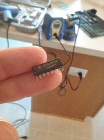
I swapped out the LS367 chip...
20170610_163211.jpg

Problem solved! Thanks for the help along the way!
20170610_162323.jpg
 
Top